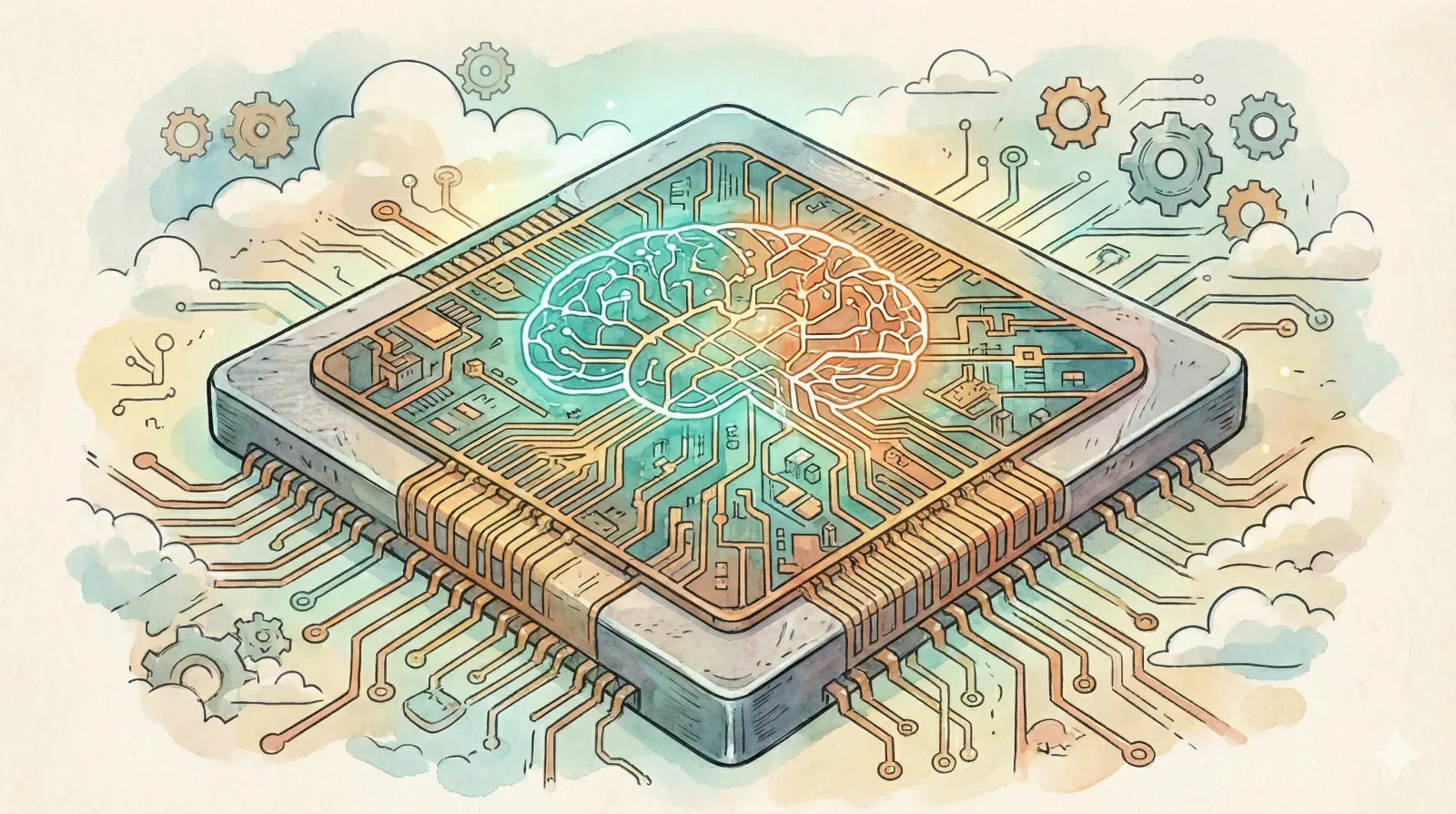
NVIDIA Built the Most Powerful Chips Ever. Google Trained the World's Best AI Without Them.
In 2020, NVIDIA released the A100 with 54 billion transistors, 80GB of memory, and 2 TB/s bandwidth. It was VERY BIG and VERY FAST(tm).
In 2022, the H100 arrived with 80 billion transistors, the first Transformer Engine optimized for the neural network architecture behind ChatGPT, and performance gains that made the A100 look quaint.
By 2025, the B200 pushed to 208 billion transistors across a dual-chiplet design, 192GB of HBM3e memory, 8 TB/s bandwidth, and support for FP4 precision that delivers 15x the inference performance of its predecessor.
This is a 2,315% increase in transistor count in five years. Memory capacity grew 140%. Bandwidth quadrupled. In less time than it takes for a good Gouda to age, NVIDIA redefined what "possible" meant for AI hardware, generation after generation.
On November 18, 2025, Google released Gemini 3. It immediately topped the Artificial Analysis Intelligence Index, LMArena rankings across text, vision, and coding, and scored 91.9% on GPQA Diamond (PhD-level science reasoning). On MathArena Apex, it jumped from 0.5% to 23.4%—a 46x improvement over Gemini 2.5 Pro.
The training infrastructure for this achievement? Google's own TPUs. According to the Gemini 3 Pro Model Card, training was done using JAX and ML Pathways on TPU infrastructure. Not a single NVIDIA chip involved.
The Myth of the Moat
For three years, the prevailing wisdom in AI infrastructure was simple: NVIDIA or nothing. Primarily running in a single box (though clustered too!), using the CUDA ecosystem, the software tooling, the whole bit. The combination of all these things were described as insurmountable moats. Startups measured their credibility by A100 count. "Stack more GPUs" became a reason to get funded.
But it was never a law of the universe, it was a supply chain dependency dressed up as technical necessity.
Gemini 3 reveals what happens when an organization can design its own silicon, optimize its training frameworks (JAX, ML Pathways), and deploy directly to 2 billion monthly Search users and 650 million Gemini app users. The vertical integration isn't just efficient; it's strategically independent.
More telling: Anthropic, Google's direct competitor in foundation models, recently committed to a multi-billion dollar deal for TPU access (reportedly "tens of billions of dollars" for "as much as a million" TPUs over the coming years). Apple, OpenAI, and Meta are all testing or actively using TPU infrastructure. The companies building the most capable AI systems in the world are diversifying away from NVIDIA dependency.
What Actually Changed
The B200's specifications are genuinely impressive. Fifth-generation NVLink connects up to 576 GPUs. The dual-chiplet architecture packs more transistors than seemed manufacturable. FP4 precision enables inference workloads that would have been impractical two years ago.
But Google's TPU v6 wasn't designed to match NVIDIA's specs. It was designed to train transformers efficiently at Google's scale, on Google's infrastructure, with Google's software stack. Different optimization target, different result.
This distinction matters more than the benchmark numbers. NVIDIA builds general-purpose accelerators sold to anyone with budget. Google builds purpose-specific silicon for its own workloads. The B200 has to be good at everything; TPUs only need to be exceptional at what Google actually runs.
When you control the entire stack - chip architecture, training framework, model design, and distribution - you can make tradeoffs that merchant silicon vendors cannot. Google's engineers aren't constrained by what the market demands. They're constrained by what Google needs.
The Coming Fragmentation
This isn't the end of NVIDIA's dominance. It's the beginning of hardware fragmentation by workload.
TPUs optimized for transformer training. NVIDIA's inference-focused FP4 capabilities. Apple Silicon optimized for on-device model execution. Amazon's Trainium and Inferentia for specific AWS workloads. Each architecture makes different tradeoffs for different use cases.
The "general-purpose GPU" era isn't dying, but it IS being supplemented by purpose-built silicon that outperforms it on specific tasks. The question enterprises should ask isn't "which GPU?" but "what's my workload, and who should control my silicon?"
For organizations running inference at scale, NVIDIA's Blackwell architecture offers compelling price-performance. For those training foundation models, the calculus depends heavily on scale, timeline, and willingness to invest in framework adaptation. For companies whose AI workloads are deeply embedded in specific cloud ecosystems, the native accelerators increasingly make sense.
The Data Locality Connection
There's a deeper pattern here that connects to everything I've been writing about distributed systems.
Chips SHOULD specialize for tons of reasons. For power efficiency. For thermal management. For specific precision formats. They increasingly need to be matched to workloads at design time. You can't efficiently move data to a chip optimized for the wrong task. The silicon itself encodes assumptions about what data will arrive and how it will be processed.
This inverts the traditional model. Instead of "move data to the most powerful compute," the economics shift toward "place specialized compute near the data it's designed to process." Edge inference chips. Regional training clusters. Purpose-built accelerators matched to specific data types and access patterns.
The Gemini announcement isn't primarily about TPUs beating GPUs. It's a proof point that the "NVIDIA or nothing" constraint was always organizational (or software based!), not physical. Organizations with sufficient scale and integration depth can build exactly what they need.
For everyone else, the lesson is different: understand your actual workload, question vendor lock-in assumptions, and recognize that the next five years of AI hardware will likely look a lot different than the last five.
What This Means
The team at NVidia built something remarkable. The A100 to B200 trajectory represents engineering at the edge of what's manufacturable. NVIDIA's market position remains formidable, and will for the foreseeable future.
But Google demonstrated that market position and technical necessity are different things. The most capable AI model in the world, by multiple independent benchmarks, runs on silicon that NVIDIA had no part in creating.
The AI hardware landscape is fragmenting. The question isn't whether specialized silicon will matter; it already does. The question is whether your organization's AI strategy accounts for a world where "GPU" is no longer synonymous with "generic tensor engine," and where the chip your workload runs on might be designed by your cloud provider, your device manufacturer, or eventually, your own engineering team.
The 208 billion transistors in the B200 are impressive. But they're not the only path forward. Google just proved it.
Want to learn how intelligent data pipelines can reduce your AI costs? Check out Expanso. Or don't. Who am I to tell you what to do.*
NOTE: I'm currently writing a book based on what I have seen about the real-world challenges of data preparation for machine learning, focusing on operational, compliance, and cost. I'd love to hear your thoughts!